Services
Click on the links below
> Home
> About us
> Industrial Sectors
> Courses
> Expert Witness
> Failure Analysis
and
Root Cause Analysis
> Testing & Evaluation:
-
Inhibitor Laboratory
&
Field Testing
-
Corrosion Mapping
-
Electrochemical
-
Metallurgical
-
SEM, XPS etc
> Publications:
- Book
- Patents
- Papers and
- Conferences
- Links to other sources
of information
> Monitoring
and
Data Interpretation
> Asset Integrity
> Innovation:
- Research & Development
- CMC Equipment
> People
>
Clients
>
Contact us
|
S
canning
R
eference
E
lectrode
T
echnique
:
Examples of of colour maps obtained. |
|
Reference on Scanning Reference Electrode Technique by CMC staff:
P.S. Sidky: Proceedings of Corrosion & Environment Conference (1998), Bath, UK, pages 185-201.
|
|
Potential
|
|
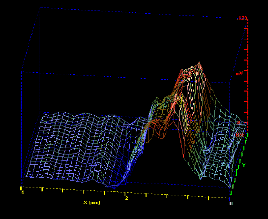
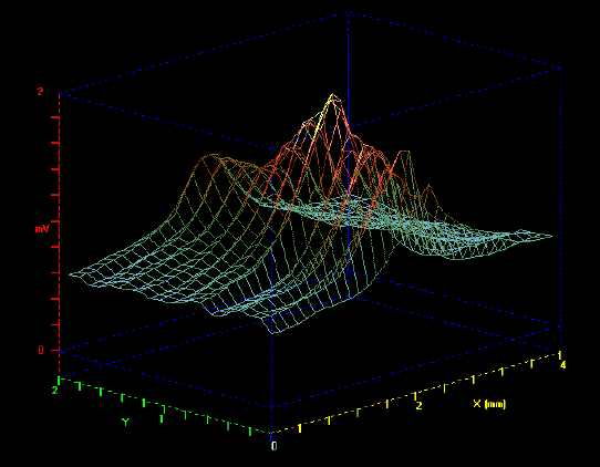
These scans are of the field
(i.e. potential gradient dV/dz, proportional to current ) over the same specimen whose potential scan is shown above.
Note the amount of detail; scan is
rotated
to reveal detail.
The field ranges from -0.03 to 0.129 mV/micron
on Z-axis (red). |
|
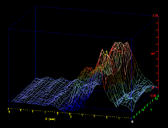
Same field scan,
rotated slightly
These scans show the vertical field but the
horizontal fields dV/dx and dV/dy are also plottable from the scan data collected.
So
horizontal currents
can also be obtained.
|
|
Potential scan across 1 mm scratch on
painted steel in 0.035% NaCl, after 26 hours
1 mV plot resolution.
|
|
Potential scan across 1 mm wide
scratch on coaltar epoxy painted steel in 3% NaCl.
0.7 mV span
1 microvolt plot
resolution. |
|
Same specimen
3 hours later
2 mV span on
z-axis
1 microvolt
plot resolution. |
|
Same specimen
after 4 hours
2 mV span on
z-axis
1 microvolt
plot resolution. |
|
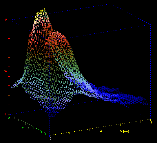
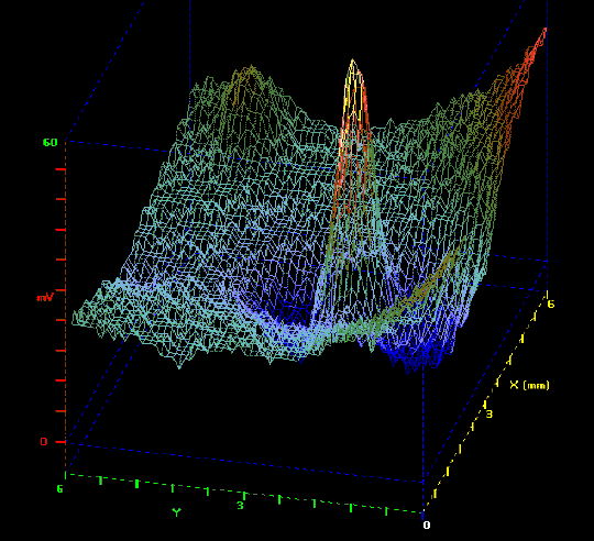
Potential scan
over pit in an unpainted stainless steel
60 mV span on
z-axis
1 mV plot resolution
|
|
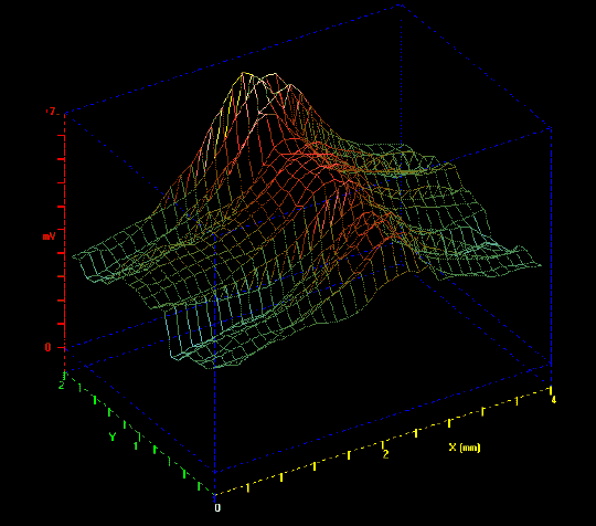
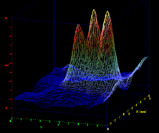
Potential scan
over pits in another unpainted stainless steel
6 mV span on
z-axis
20 microvolt
plot resolution
|
|
CURRENT MODE MEASUREMENTS:
A "Point-In-Space" calibration graph is required to obtain current values.
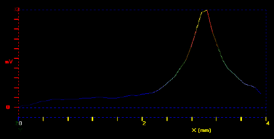
A linear scan is made over a 70 micron dia. vertically-mounted wire with 4 microamps passing from it to a large Cu anode. Maximum potential with probe directly over wire tip is 3 mV and peak width at half-maximum is 0.6 mm. A plot of potential vs current is linear over this point. |
|
ADVANTAGES over SVET scanners:-
Gives
vertical
and
horizontal currents
(SVET only gives vertical current component).
Also gives
potentials
(SVET only gives currents).
Absence of vibratory stirring
allows sharp resolution of defects (SVET has a vibrating electrode).
Unique feature:
Automatic probe contouring
allows scanning of non-flat surfaces
such as weld beads and
paint blisters (SVET requires a flat surface and its probe is damaged if it contacts a surface).
No need to fix specimens accurately horizontal
, so results are independent of operator skill.
Your own probe can be used, allowing experimentation with extra-narrow probe tips for the experimenter.
|
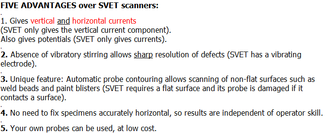
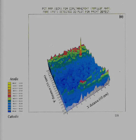
potential scan
over a pitted
stainless steel
Potential vs
distance (X & Y) map.
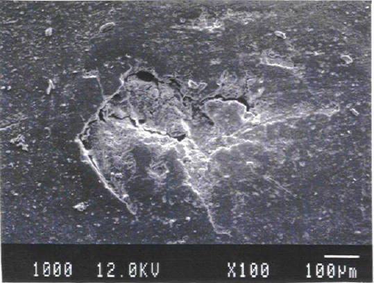
The paint defect, seen as a peak, is shown in an SEM photograph below.
Field
Field
|
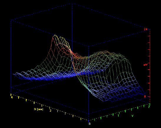
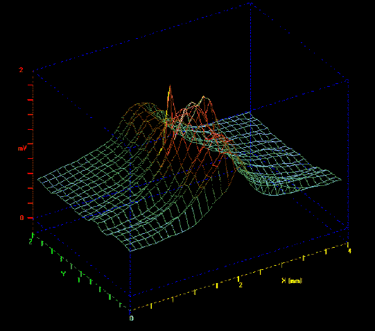
This scan is of the electrochemical
potential over a scratched painted steel surface in 3% NaCl, with the 1 mm scratch parallel to the y-axis and located at x = 1.3 mm. The scan shows that the scratch region nearest to y = 0 is more anodic than the rest. The corresponding field scan, proportional to the current from the scratch is shown next below this one, rotated to different angles. All scans can be rotated and tipped, in 1º steps. Plot resolution is 1 mV |
|
PROFILOMETER MODE
. NOTE: This picture is much sharper (higher resolution) than shown here in this small copy. |